Topic
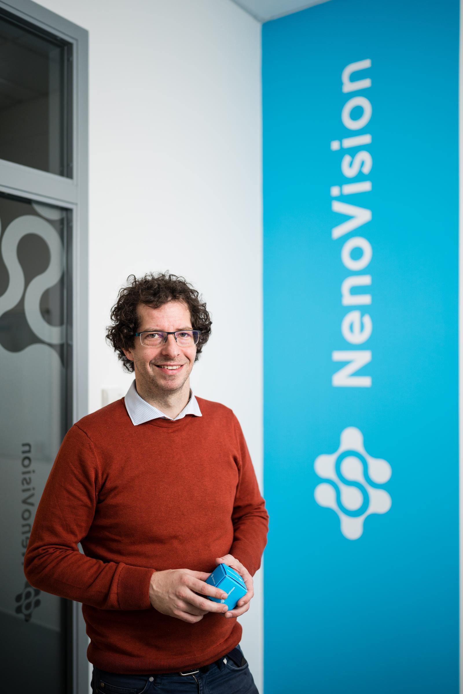
From a student project to a successful international company. NenoVision co-founder Jan Neuman urges students not to let their ideas sleep in a university drawer
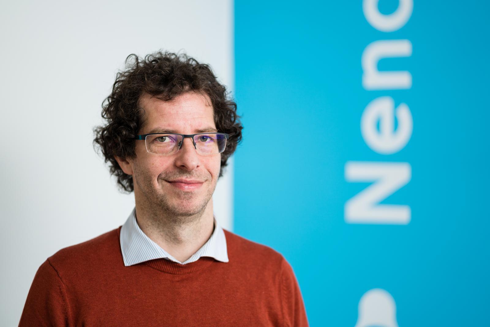
He felt it made more sense than discovering a hole in the market. Jan Neuman, a graduate of the BUT's Faculty of Mechanical Engineering, used a stand-alone atomic force microscope (AFM) and an equally powerful scanning electron microscope (SEM) to measure surfaces. He moved the sample back and forth between them because he needed to characterise it with both techniques. It was then that he realised the advantage of linking the two devices, which he and two other PhD students were working on. After five years, they managed to build an atomic force microscope that integrates into an electron microscope, and later decided to go to market with it. NenoVision became the first ever spin-off company of CEITEC BUT. It celebrated its seventh anniversary this November.
How did the idea of combining atomic force techniques with the electron microscope come about?
Before we founded NenoVision, my colleagues Zdeněk Nováček and Michal Pavera and I were doing our PhDs under Professor Tomáš Šikola. During the studies, a large project funded by the TAČR was being prepared and the professor together with the director of Tescan, Jaroslav Klíma, came up with the ambitious idea of integrating atomic force microscopy technology into a specialized electron microscope and wrote it into the project. The idea passed and we took it upon ourselves to implement it. We developed the first version over five years and by the end of the project we had succeeded. We had a working prototype that took the first pictures. This began our adventurous journey, whose patron was Professor Šikola, who supported us students and believed in us, for which we owe him a huge thank you. We also received other help, but we will get to that.
Why did you initially decide to commercialize the student project?
I always wanted to be an entrepreneur. I wasn't too keen on the idea of my output being just an article. I don't have the necessary scientific zeal for that. I needed a result that would be tangible and useful to other people. In fact, I was and still am sad that so many great ideas, technologies and products are produced at the university but remain "in the drawer". I would like to tell all students to take a risk, because when else but now? Let them take what they've been working on and take it to market! I'll be happy to help them, and so will dozens of other people in the South Moravian Innovation Centre (JIC) or in the whole Brno microscopy community. Just one phone call.
That's very motivating and sounds easy. I suppose it was more complicated than that. What steps preceded the establishment of NenoVision?
The decision was terribly difficult because you are going to take a huge risk. You don't know who would buy it and whether it would succeed, but we thought if it didn’t, we had the opportunity to apply for a job at Tescan, Thermo Fisher or Delong, so we took the plunge. We knew from the beginning that we were building a facility that would be for very few customers – only those who worked with specialized electron microscopes (such as in the ultravacuum). So, we decided to rebuild our product a bit into an accessory for conventional electron microscopes. With the help of JIC, we then followed up with a market analysis of how many such microscopes there are, how many we could sell, and based on that we decided to give it a try. In November 2015, we founded NenoVision.
Where did you get your information on how to take university know-how and transfer it to a commercial environment?
In the beginning there was a great collaboration with the aforementioned Professor Šikola, who helped us and supported us fully. I was still working as a project manager of the start-up CEITEC centre during my PhD and then I was in charge of the science and research support department where we dealt with spin-off companies and transfers. So, it was nothing new for me, we agreed with the university on the terms and conditions and the royalty, which is actually a percentage of the sales. It was significantly more complicated to change our mentality from university to corporate. That's a huge difference. At university you want to research, research something completely new, develop something and write the best paper you can. At a company, it's different. There has to be a product at the end that someone will pay for. You have to make dozens of decisions to get somewhere. We started shifting to a corporate mentality right from the beginning, but it wasn't until about a year or two ago that I think we started to get it right. Now we have our company goals set commercially and we share them in the company. We know what our vision is and where we are going.
Did you have someone helping you with that?
The South Moravian Innovation Centre. We've been coming here since the beginning; we've been through various programmes and had several mentors. We learned how to prepare a business plan, how to get investors. Then they also helped us with ownership, financial plans and building a business network. We don't know, we'll call and they'll guide us or recommend a program. JIC is a great organization with inspiring people who are willing to help. It's a pretty unique ecosystem and a warm hand extended to anyone who wants to initiate a start-up in South Moravia. JIC has managed to build a functioning community of professionals across industries and companies who help each other. The whole microscopic environment in Brno has also been very supportive. There are people there who have been in this business all their lives, and that is reflected in the group. Nobody closes the door on you, nobody asks what they're going to get in return. The energy is great and energizing. Now we're trying to give back to that community. For example, I've already consulted about 20 people on ideas.
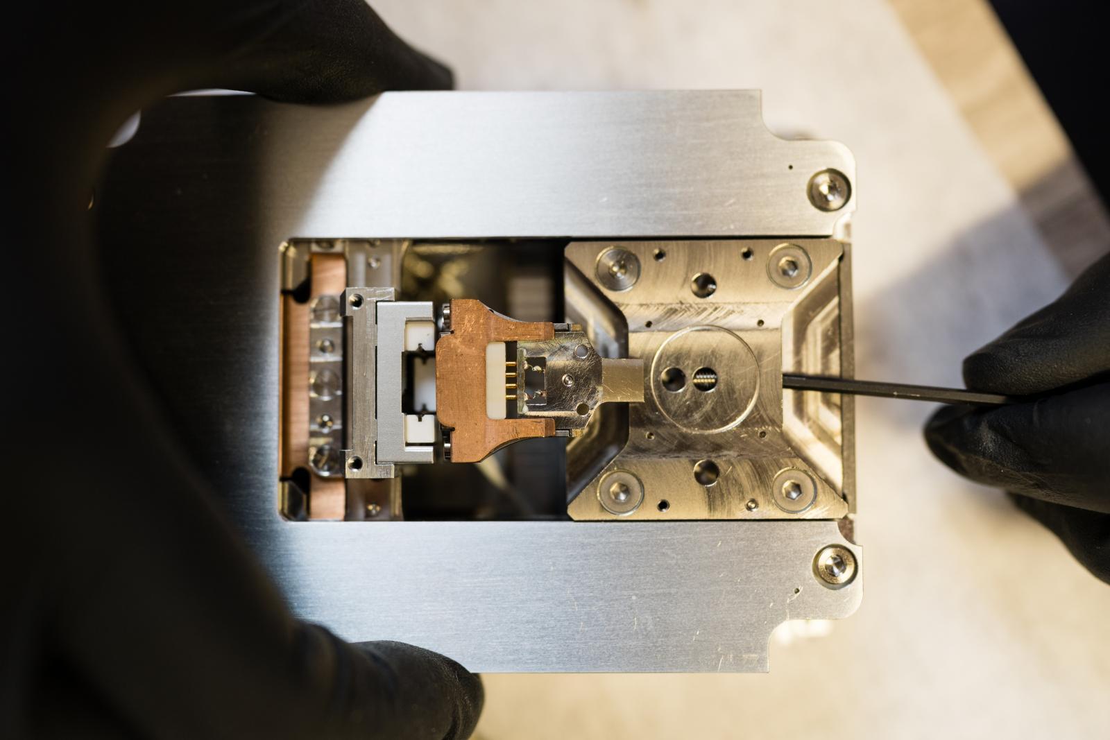
So, you came to market with LiteScope, an atomic force microscope that connects to an electron microscope. What followed?
It's important to say that atomic force microscopy (AFM) is a very established technique. It is one of the standard methods for materials science. And so is scanning electron microscopy (SEM). The stand-alone AFM and SEM communities are huge. And what we've done is we've combined the advantages of both techniques. The biggest piece of work was, and still is, to show the world how the combination is good and indispensable. When you come to market with a new technique, you are testing the demand and at the same time opening up questions in the scientific community about what it would be for and for whom. So, for seven years we've been actively touring conferences, universities, doing webinars, educating the community, showing the benefits of our technology and trying to inspire others to think about how they could use it. And it's terribly challenging because we're building a market and changing the way people look at microscopes and what can be done with them. It's just that people are working in familiar patterns, so it's a long haul. You're putting a lot of energy into it, and it takes three, four years to get the payback. I'm very happy that we're reaping the rewards lately. We're getting a lot more awareness and interest in our technology.
How many times during that marathon did you tell yourself that you couldn't run anymore?
It depends. One of the co-founders, Z. Novacek, said last January that he was in over his head, so he quit and went back to university. It can be stressful and frustrating. You work, you work, and the results are not coming in yet. I personally had a crisis two years ago. I felt that the atmosphere in the company was not good. I was tired and frustrated and wondered if it was all worth it, but then Eva Vacíková started helping us with HR stuff and development within the company. And since then, a lot of things have changed and we're functioning very differently. For the last year and a half, the atmosphere has been great and we're also getting positive feedback from customers and people we work with – ETH Zurich, KIT and BASF in Germany. We have installations in Italy, Germany, Hungary, France, China and other countries, including our home country, where there are around five installations. One at CEITEC BUT so we get feedback personally right in our homeland, and at the same time we have partners here with whom we further develop and improve our product. So, I'm very proud of how far we've come. Plus, we have great colleagues and students who come up with new ideas. That's very fulfilling for me.
So, you were three co-founders at the beginning. How many are there now?
Now we are 18 plus about 6 students, which is fantastic because we are still working with CEITEC and BUT. Students do their bachelor's and master's theses with us and often stay with us. They bring new energy, ideas, and still do a good job.
Where has NenoVision moved to?
From the beginning, we have worked along two lines. The first was in device development, and the second was in discovery – learning what the customer needed, what our LiteScope device could be used for, and constantly going out and building a business network, partners and distributors. In both spheres, we have grown significantly. The product is stable and no longer has any "childhood diseases". We also already know what areas of application we want to focus on and where the greatest potential is. We are now working with some twenty giants in materials research across the world, which is driving us forward significantly.
What did LiteScope do then and what does it do now?
Initially, it was great at measuring one thing, and that was topography. So, at the nanometre level, LiteScope allowed us to see what the relief of a sample looked like, which an electron microscope can't do. Over time, we added other techniques that are common to atomic force microscopy. So today it can measure the electrical, mechanical, chemical and magnetic properties of materials. We are the leaders in this field. We also offer our CPEM technology, which makes us the only company in the world that can simultaneously measure with an atomic force microscope and an electron microscope. This is called correlative microscopy, which is also the "driver" of our business.
Would you explain how both types of microscopes – SEM and AFM – work?
I have a great analogy for that. I'm going to use our two senses – sight and touch. I have a coffee mug on my desk. If I want to know something about it, I look at it first to find out its size and shape, but if I want to find out if it's soft rubber or hard ceramic, I have to touch it. My eyes can't help me. In this case, the electron microscope is sight and the atomic force microscope, where I have a sharp tip that I touch the material with, is touch. And it's advantageous to use both senses. Using the "eyes" of the electron microscope, I spot the spot I am interested in and send my "hands", the tip of the atomic force microscope, there to measure the spot.
What target group are you aiming at?
Today's customers are mainly universities and research institutions that do materials science. There, our equipment has huge potential applications. Looking to the future, we have chosen three main areas that are related to global sustainability. Something where we all feel that science and microscopy must intervene. So, we did a workshop on what NenoVision can do to help with sustainability and reducing emissions. How our equipment can help and in what areas. And from that we started to "look at" solar cells, batteries, semiconductor components or sustainable materials. All of which we can improve with the LiteScope microscope – increasing their efficiency or lifetime or reducing energy consumption. We also want to focus on "life science". Here, our device could be a breakthrough for many discoveries. So, we want to move from basic research to high-tech industrial applications.
From what you say, I get the feeling that LiteScope has almost unlimited applications. What percentage of its potential have you already exploited?
I think we have found a use for about 10 % of its potential. We know about another 40 % of the possible applications and areas of use, and the remaining half remains to be discovered. There are an incredible number of doors opening up here and we are now choosing which ones to enter. There are so many ideas of what to do and where to go. The most important thing for us is "impact", what application will have the greatest use and whether it fulfils the areas and visions we have set out.
So, let me ask you another way, what can't you do with it?
Our technology has about a thousand limitations from the physical principle of how it works. For example, by running a sharp point on a surface, you never look inside. And that's why it's useful to combine our technique with, say, a CT scanner. We're back to correlative microscopy. The stacking of different imaging techniques is proving to be crucial in the characterisation of batteries, semiconductor components, for example. First, CT is used to find areas that are "suspect", then the battery or semiconductor is cut and our equipment is used to measure these problem areas in detail.
What are your future plans?
We will be launching a new generation of our device shortly and we are already talking about what it will look like in three years' time. We're looking significantly more at what the applications we want to develop need and what we need to develop for them. For example, we plan to use artificial intelligence to automatically process images. We want a person to just press a button and that would trigger a measurement, where parameters would be automatically adjusted according to what the sample looks like. This would, of course, open the door to routine quality control in high-tech industries and other sectors. To summarise, we would like to continuously push the boundaries of correlative microscopy and use it for real-world applications, such as the aforementioned battery life extension. This allows us to pause occasionally on our challenging journey and realize that the results of our work are actually helping someone.
An Italian couple from CEITEC BUT succeed with research on the capture of nanoplastics by MXene microrobots
Science is made by people and people are driven by passion. However, passion alone is not enough, says Vinicius Santana
Scanning zebrafish for microplastics: Micro-CT as a non-destructive way to image microplastics in biological samples
Ordered nanocrystal ensemble that degrades pollutants using light. Meet Brno PhD Talent winner Anjali Valadi Palliyalil
CEITEC scientist creates 3D model of a rare cave-dwelling salamander to facilitate its research